NVIDIA GeForce GTX 280 and GTX 260 Unleashed

Unlike the initial G92 launch with the GeForce 8800 GT, where we were left with questions regarding the total number of stream processors and texture units inside the GPU, with today's GT200 launch there are no such questions. The die shot below clearly shows the ten banks of 24 stream processor clusters. Count them yourself if you'd like verification.
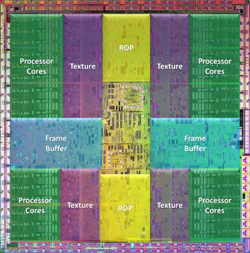
;) What you're looking at here is a 1.4 billion transistor GPU, produced on TSMC's 65nm process node. As the overlay shows, the stream processor clusters, texture units, ROPs, and frame buffer memory partitions are all segmented and spread out across the entire GPU. We should note, that the GT200 is the largest, most complex chip TSMC has ever manufactured. The wafer shot to the left here shows just how big the GT200 is, and also hints to to fact this this is going to be an expensive part to produce. If you count the number of full dies on that wafer, you'll see there are only 94 complete units. In addition, the edge die that get chopped and wasted in the circular shaped of the wafer, are numerous. Then account for defects and of course that number only goes down. Although they haven't officially acknowledged it just yet, just looking at that wafer it's highly likely that NVIDIA has plans to shrink this GPU architecture ASAP. 45nm would do this chip a whole lot of justice.
What you're looking at here is a 1.4 billion transistor GPU, produced on TSMC's 65nm process node. As the overlay shows, the stream processor clusters, texture units, ROPs, and frame buffer memory partitions are all segmented and spread out across the entire GPU. We should note, that the GT200 is the largest, most complex chip TSMC has ever manufactured. The wafer shot to the left here shows just how big the GT200 is, and also hints to to fact this this is going to be an expensive part to produce. If you count the number of full dies on that wafer, you'll see there are only 94 complete units. In addition, the edge die that get chopped and wasted in the circular shaped of the wafer, are numerous. Then account for defects and of course that number only goes down. Although they haven't officially acknowledged it just yet, just looking at that wafer it's highly likely that NVIDIA has plans to shrink this GPU architecture ASAP. 45nm would do this chip a whole lot of justice.
And although the GT200 does borrow heavily from G80 / G92 architectures, there are some significant enhancements here, over and above the increased number of stream processing units. The GT200 for example, supports three times the number of threads in flight as the G80 at any given time. It also has a new scheduler design this is up to 20% more efficient. The GT200 also supports a wider 512-bit memory interface and has improved z-cull and compression technology. This new GPU has more aggressive clock gating and power saving technology built-in too, which results in significantly lower idle power usage than you might expect and it support's NVIDIA's HybridPower feature as well.
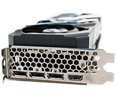
Unlike the G80 which performed ROP frame buffer blending at half speed, the GT200 can perform the same tasks at full-speed. The GT200 GPU also sports twice the number of registers for longer, more complex shaders. The chip's output buffer size has been increased by a factor of six and it offers IEEE 754R compliant double precision for improved floating-point accuracy. And although the first crop of cards based on the GT200 are equipped with DVI outputs that won't exploit it, the GPU has hardware support for 10-bit color scan out as well, but it'll need a DisplayPort interface to use it.

GT200 GPU Block Diagram - Graphics Mode Configuration
The high-level block diagram above represents the GT200 GPU operating in graphics mode on a GeForce 280 GTX. The shader thread dispatch logic is located at the top along with the setup and raster units. The ten thread processor clusters each include three groups of eight stream processors for a total of 24 processing cores per cluster. Multiply that by ten and you have a grand total of 240 scalar processing cores. ROPs (raster operations processors) and memory interface units are located at the bottom. The ROPs can deliver a maximum of 32 pixels per clock, which equates to 4 pixels per clock, per ROP partition, times eight partitions. We should also note that up to 32 color and Z samples per clock for 8X MSAA are supported per ROP partition as well. The 512-bit wide memory controller is partitioned into eight segments, with two chunks of memory connected to each segment.
The GT200 is implemented differently on the new GeForce GTX 260, however. On the GTX 260, two of the thread processor clusters and one of the memory partitions are disabled, for a total of 192 active SP units and a 448-bit memory interface, with 14 pieces of memory.

GT200 GPU Block Diagram - Compute Mode Configuration
The high-level diagram above is representative of the GT200 GPU operating in compute mode. The hardware-based thread scheduler at the top manages the scheduling of threads across the thread processor clusters. In compute mode, the texture caches are used to combine memory accesses for more efficient and higher bandwidth memory read / write operations. And while the ROPs are out of the picture, there are some new elements, called "Atomic", visible. The Atomics refer to the ability to perform atomic read-modify-write operations to memory. The Atomics provide granular access to memory and facilitate parallel reductions and parallel data structure management.
We should note, that the GPU cannot operate in both modes simultaneously - it is either in compute mode or 3D graphics mode. When PhysX support comes in a future driver release, for example, CUDA compatible GPUs like the GT200 (G80 and G92) can be used as a 3D accelerator or a PhysX accelerator at any given time, but not both simultaneously. The GPU must switch states depending on the type of workload.