AMD Sempron 3400+ Launch
Introduction and Product Specifications
![]()
For years, AMD has been a growing thorn in Intel's side. Early on, AMD had a much smaller market share than the elder silicon giant, but as the years progressed, AMD's foothold grew. By continually introducing new products that compete directly with Intel's product line, AMD has grown to be a formidable foe for the incumbent chip maker. Fast forward to today and you have a thriving company that not only competes on the same level as Intel, but manages to surpass them in many respects.
In July 2004, AMD added the budget CPU sector to their hit list, taking on Intel's Celeron line with the Socket A based Sempron 2800+ and Socket 754 based 3100+. Then in April 2005, AMD added to the Sempron line with the 3300+ socket 754 which was produced using a refined 90nm manufacturing process. Designed to take on the fastest Celeron processors available at the time, then clocked at 2.8GHz, the 2GHz Sempron 3300+ beat the Celeron hands down in the majority of tests. Now, less than four months later, AMD delivers their first budget 64-Bit processor in the form of the Sempron 3400+. With 256KB of L2 cache, 128KB of L1 cache and running at 2GHz, the Sempron 3400+ aims to stay on top of the budget CPU sector with its performance and features.
We should note that Intel technically beat AMD to the 64-Bit punch in the budget CPu segment, with the release of the 64-Bit Celeron D line on June 27th. However, as of the writing of this article, availability of the 64-Bit Celeron D's is limited, as several of the larger online retailers are not currently offering Intel's 64-Bit Celeron D. So, at this time no performance scores were included but we hope to update this in the not-to-distant future.
|
;) Model / Frequency / Cache: 3400+ / 2.0GHz / 256KB L2 cache (and standard 128KB L1 cache) CPU to Memory Controller: 2.0GHz Memory Controller: Integrated 64-bit wide memory controller Types of Memory: PC1600, PC2100, PC2700 and PC3200 DDR unbuffered memory HyperTransport Links: 1 HyperTransport Spec: 1.6GHz (2x 800MHz / DDR) Effective data bandwidth: 9.6GB/sec [6.4GB/sec x1 HyperTransport link + 3.2GB/sec memory bandwidth] Packaging: |
Fab location: |
;)
When we line up the Sempron product line side-by-side, the differences are easier to discern. The like the 3300+, the Sempron 3400+ is built on their 90nm manufacturing process. When AMD made the move the Sempron to their 90nm line, they not only introduced SSE3 instruction support to the Sempron line, but AMD also implemented changes to the memory controller as well. These enhancements improved both memory mapping and memory loading while adding support for mismatched DIMMs.
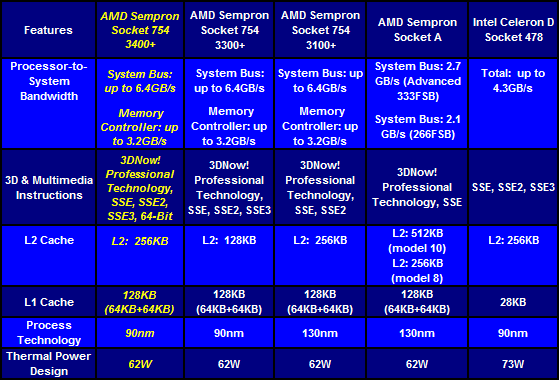
The major "physical" difference between the Sempron 3300+ and 3400+ is the 3400+'s 256KBof L2 cache compared to the Sempron 3300+'s 128KB L2 cache. Each processor shares the same 2GHz clock speed, 128KB L1 cache and memory bandwidth. The biggest "feature" difference is the added support for 64-Bit computing with the Sempron 3400+. The 64-Bit ready Semprons are identifiable by the last two characters in the OPN. If the processor OPN ends with "BO" or "BX", this designates the processor as a 90nm, 754 Pin x86-64 Sempron Processor. With Commercial PC's utilizing a 64-Bit Sempron processor, manufacturers will clearly mark the machines as having a Sempron with AMD64 Technology.


