AMD Sempron 3300+ Launch
Introduction to the Sempron 3300+
![]()
In July of 2004, AMD released their latest economy class processors in the form of the Sempron line. The initial release was predominantly Socket A-centric, with only one Socket 754 solution being offered. Since that day, the Socket A Sempron family has grown to incorporate 7 flavors, yet the socket 754 Sempron line only recently added a 3000+ to the mix.
This morning AMD has taken the wraps off their latest edition Sempron, the Socket 754 based Sempron 3300+. Back when the Sempron 3100+ was released, Socket A models were targeted at Intel's Celeron family, while the 3100+ was in a class of its own, not matching up directly to any Celeron available on the market at that time. This time around, AMD is targeting the Celerons with their 3300+, looking to challenge the fastest Intel Celeron-D offerings currently available.
;)
;)
While some may think the Sempron 3300+ is merely a speed bump compared to the 3100+, we need to re-think that logic. AMD has tweaked the processor with new features and manufacturing process to help maintain a competitive edge in the economy CPU sector. Today, we'll highlight the critical changes that are incorporated in the latest Sempron 3300+, then we'll line up AMD's latest chip next to the 3100+ and a Celeron D 335 to see if the Sempron 3300+ lives up to AMD's marketing effort.
|
| Packaging: Socket 754:3300+ Process Technology: Memory: HyperTransport Links: Effective data bandwidth: |
FSB: Cache size: Voltage & Heat Dissipation: Frequency: Price: |
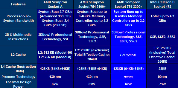
When we look at the grid above, the Sempron 3300+ brings a couple of new things to the table compared to the elder 3100+. Based on the "Palermo" core, AMD is manufacturing the 3300+ at .09 microns with half of the L2 Cache complement of the .13 micron 3100+. With 128KB of L2 cache, the Sempron 3300+ is clocked 200MHz faster than the 3100+, running at 2.0GHz. Additionally, AMD has added support for SSE3 instructions, something only the Celeron offered up until now, as far as budget CPUs go anyway.
Along with the 90nm process, AMD has tweaked the onboard memory controller of the 3300+ Sempron for more flexability and stability as well. Improvements have been made to memory loading and mapping, aiming to increase overall efficiency. Lastly, AMD has improved the memory controller to support different sized DIMMs on the same channel. Aside from these key changes, the Sempron 3300+ closely resembles the 3100+ while bringing a more competitive feature set to challenge Intel's Celeron line.
With half the L2 of both the 3100+ and Celeron line, we are curious how this CPU will shape up in the benchmarking segment. First, let us load CPU-Z to offer a visual comparison of the three processors, then we'll put the Sempron 3300+ to the test and see how it faired when we ran a wide range of benchmarks on all three chips.


