NVIDIA GeForce GTX 960 Review With EVGA And ASUS
Introduction and Specifications
To date, NVIDIA has introduced only a couple of Maxwell-based desktop GPUs. Back in September, the company launched the powerful and potent GeForce GTX 980 (and its little brother, the GeForce GTX 970), featuring the GM204. The GM204 is currently NVIDIA’s fastest single-GPU, though a larger “big” Maxwell-based chip akin to the GK110 powering cards like the GeForce GTX Titan, will likely be introduced at some point as well. Looking even further back, we first got a glimpse of Maxwell on the diminutive GeForce GTX 750 Ti. That card was based on the GM107 GPU, a smaller Maxwell variant, that targets low-power and mainstream applications.
Today, NVIDIA is going after the sweet spot of the discrete GPU market, currently occupied by cards like the GeForce GTX 760 and older GTX 660. On the following pages, we get to show you the new GeForce GTX 960, which features a brand new Maxwell-based GPU dubbed the GM206 that’s falls somewhere in between the GM107 and GM204, but features all of the goodness of both. The GM206 has all of the features of the bigger GM204 (and then some), but low-power characteristics that more closely align to NVIDIA's GM107.
Take a look...

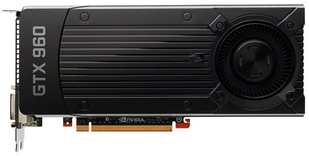
NVIDIA GeForce GTX 960 Reference Card
|
|
NVIDIA GeForce GTX 960 | ||
| Graphics Processing Clusters | 2 | |
| Streaming Multiprocessors | 8 | |
| CUDA Cores (single precision) | 1024 | |
| Texture Units | 64 | |
| ROP Units | 32 | |
| Base Clock | 1126MHz | |
| Boost Clock | 1178MHz | |
| Memory Clock (Data rate) | 7010MHz (Effective Speed - ~9300MHz) | |
| L2 Cache Size | 1024KB | |
| Total Video Memory | 2048 MB GDDR5 | |
| Memory Interface | 128-Bit | |
| Total Memory Bandwidth | 112.6 GB/s | |
| Texture Filtering Rate (Bilinear) | 72.1 GigaTexels/sec | |
| Fabrication Process | 28 nm | |
| Transistor Count | 1.94 Billion | |
| Connectors |
3 x Display Port | |
| Form Factor | Dual Slot | |
| Power Connectors | One 6-Pin | |
| Recommended Power Supply | 400 Watts | |
| Thermal Design Power (TDP) | 120 Watts | |
| Thermal Threshold | 95°C | |
| Price | $199 MSRP - Find Them At Amazon | |
The new GM206 GPU at the heart of the GeForce GTX 960 features roughly 2.94 billion transistors and has die size of 227mm2. And like its predecessors, it’s built on TSMC’s 28nm process node. It’s likely that future NVIDIA GPUs will use a more advanced manufacturing process, but for now, 28nm is it.
Like the GM204 powering the high-end GeForce GTX 980, NVIDIA was able to optimize the GM206’s power efficiency without moving to a new process, by tweaking virtually every part of the GPU. NVIDIA took what they learned with Kepler and its Tegra SoCs and put much of that knowledge into Maxwell. As we’ve mentioned in previous articles, Maxwell is designed to boost efficiency through better GPU utilization, and ultimately improve performance per watt and per die area. NVIDIA claims that Maxwell SMs (Streaming Multiprocessors) offer double the performance of GK104 and double the perf-per-watt as well. Maxwell's new scheduler architecture has not only received a number of updates to improve power efficiency, but also to enhance performance as well.
Maxwell’s Streaming Multiprocessors, or SMs, are somewhat different than Kepler’s. With Maxwell, NVIDIA has made improvements to the control logic partitions for better workload balancing, and it also has finer-grained clock-gating and better compiler-based scheduling. Maxwell can also issue more instructions per clock cycle, all of which allow the Maxwell SM (also called an SMM in some NVIDIA docs) to exceed Kepler’s SMX in terms of efficiency. NVIDIA is claiming that Maxwell’s new SM architecture can deliver 40% more performance per CUDA core on shader-limited workloads than Kepler, with up to double the performance per watt, despite using the same 28nm manufacturing process.


GM206 Block Diagrams - Click To Enlarge
The GM206 GPU contains two GPCs, eight Maxwell Streaming Multiprocessors (SM), and two 64-bit memory controller partitions (128-bit total)—it is essentially half of a GM204. Each SM is partitioned into four separate processing blocks, each with its own instruction buffer, scheduler and 32 CUDA cores. With Kepler, the control logic had to route and schedule traffic to 192 CUDA cores, which were harder to keep fully utilized. This partitioning simplifies the design and scheduling logic, saving area and power, and reduces computation latency. The compute L1 cache function has now also been combined with the texture cache function, and shared memory is a separate unit shared across all four blocks.
NVIDIA’s reference specifications for the GeForce GTX 960 call for a base clock of 1126MHz and a Boost clock of 1178MHz. The GPU is packing 1024 CUDA cores, 64 texture units, and 32 ROPs, which again, is half of what’s inside the GeForce GTX 980.
The 2GB of video memory on GeForce GTX 960 cards is clocked at a speedy 7GHz (effective GDDR5 data rate) and the memory links to the GPU via a wide 128-bit interface. At those clocks, the GeForce GTX 960 offers up a peak textured fillrate of 72.1 GTexels/s and 112 GB/s of memory bandwidth. Those numbers might seem low in light of some previous gen GeForce cards and current Radeon cards with wider memory interfaces, but NVIDIA points out that the new memory compression technology in Maxwell affords up to an additional 30% of effective bandwidth, so the max effective data rate is equivalent to about 9300MHz.
Though the GM206 is similar to the GM204 in almost every way, NVIDIA did make one addition. The GM206 has support for H.265 (HEVC) encoding and decoding. The GTX 980’s NVENC video engine offers native support for H.265 encode only, no decode. Support for other features like NVIDIA’s Voxel Global Illumination (VXGI), Multi-Frame sampled AA (MFAA), and Dynamic Super Resolution (DSR) are all present on the GeForce GTX 960, as is support Microsoft’s upcoming DirectX 12 API. Since we’ve already talked about all of these features in detail in our GeForce GTX 980 launch coverage, we won’t rehash that here. If you’d like to learn more about them, we’d suggest taking a look at this article. Let's look at the cards...


