AMD Beema and Mullins Low Power 2014 APUs Tested
Introduction To Beema and Mullins
A couple of weeks back, we got the chance to get some hands on time with AMD’s upcoming mainstream and low-power APUs (Accelerated Processing Units), codenamed Beema and Mullins. These APUs are the successors to last year’s Temash and Kabini APUs, which powered an array of small form factor and mobile platforms. With this release, however, AMD was laser focused on improving power consumption and efficiency, expanding the platform’s capabilities through both hardware and software tweaks, and of course improving performance over the previous generation.
Beema and Mullins are based on the same piece of silicon, but will target different market segments. Beema is the mainstream part that will find its way into affordable notebook, small form factor systems, and mobile devices. Mullins, however, is a much lower-power derivative, designed for tablets and convertible systems. Both Beema and Mullins feature multiple SKUs, with products in the E1, A4, A6, and A10 family of APUs.
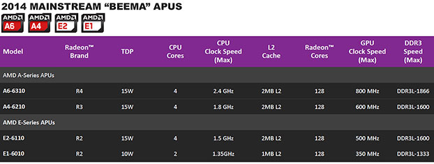
AMD is announcing four Beema-based mainstream APUs today, with TDPs ranging from 10W – 15W. The A6-3610, A4-6210, and E2-6110 are quad-core parts with 2MB of L2 cache, though they’ll feature different max core clocks and DDR3 memory speeds. The E2-6010 is a dual-core part with only 1MB of L2.
There are three Mullins-based products being announced, two quad-cores and a dual-core. The top of the line-up is the A10 Micro-6700T. It’s a quad-core chip, with a max clock speed of 2.2GHz, 2MB of L2, and a TDP of only 4.5W. The A10-6700T is the chip we were actually able to test and have a full batch of benchmarks scores for on the pages ahead. The A4 Micro-6400T is also a quad-core part, but its max CPU frequency tops out at 1.6GHz. The E1 Micro-6100T is the lowest-power part with a TDP of only 3.95W, but unlike the others it is a dual-core chip.
One thing you may have noticed looking at both of the tables above is that all of the APUs based on Beema and Mullins feature 128 (GCN-based) Radeon cores, despite the fact that they have Radeon R2, R3, R4, and R6 branding. In lieu of altering the GPU configuration, AMD differentiates the graphics capabilities of each part only by altering the GPU clock.
We’ll have more details on the changes and new features introduced with Beema and Mullins on the next page, but in a nutshell they feature updated Puma+ x86 Cores, GCN-based graphics, new System-Aware Power Management, a new ARM-based Platform Security Processor, and support for DDR3 memory speeds up to 1866MHz.
The die shot and map above illustrate Beema/Mullins’ layout. As you can see, the Puma+ X86 cores and graphics engine encompass the bulk of the center of the chip, with cache and other functional blocks surrounding them. The small yellow section labeled PSP is the new platform security processor. The PSP is a 32-bit ARM Cortex A5 core with isolated ROM and SRAM. It’s designed to function in Trusted Execution Environment (TEE), with secure boot rooted in hardware, and support for cryptographic acceleration.

AMD Beema / Mullins Functional View
These latest AMD APUs aren’t strictly CPU and GPU cores crammed onto a single piece of silicon. They are full SoCs with on-die memory controllers, PCI Express, SATA, and USB connectivity, and a host of other interface elements. Connect one of these APUs to some memory and storage, and some I/O ports and you’ve essentially got a complete low-power, X86 compatible platform, with modern Radeon graphics.


