NVIDIA GeForce GTX 760 Mainstream GPU Review
Introduction and Specifications
NVIDIA is launching yet another new member of the GeForce GTX 700 series today, the freshly minted GeForce GTX 760. Like the GeForce GTX 770 which arrived just a few weeks ago, the new GeForce GTX 760 is built around the company’s GK104 GPU—the very same chip used last year’s GeForce GTX 680 and a few other GTX 600 series cards. The GeForce GTX 760, however, targets a different market segment and is debuting at a much more palatable price point than its predecessors.
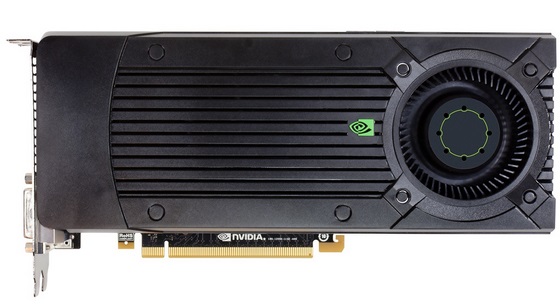
We’ve got a couple of GeForce GTX 760 cards on hand to show you here, a reference model that came straight from NVIDIA and a fully custom, factory overclocked version from EVGA, the GeForce GTX 760 Super Clocked with ACX cooling. Though, as you’ll see, while the two cards are physically very different, they perform within a few percentage points of one another. Let’s get acquainted with the reference card first and then we’ll move to EVGA’s custom offering and check out all of the performance data...
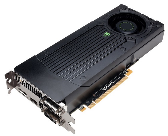
NVIDIA's Reference GeForce GTX 760
|
| Graphics Processing Clusters | 3 or 4 |
| Streaming Multiprocessors | 6 |
| CUDA Cores (single precision) | 1152 |
| CUDA Cores (double precision) | -- |
| Texture Units | 96 |
| ROP Units | 32 |
| Base Clock | 980 MHz |
| Boost Clock | 1033 MHz |
| Memory Clock (Data rate) | 6008 MHz |
| L2 Cache Size | 512 KB |
| Total Video Memory | 2048MB GDDR5 |
| Memory Interface | 256-bit |
| Total Memory Bandwidth | 192.26 GB/s |
| Texture Filtering Rate (Bilinear) | 94.1 GigaTexels/sec |
| Fabrication Process | 28 nm |
| Transistor Count | 3.54 Billion |
| Connectors |
2 x Dual-Link DVI |
| Form Factor | Dual Slot |
| Power Connectors | 2 x 6-pin |
| Recommended Power Supply | 500 Watts |
| Thermal Design Power (TDP) | 170 Watts |
| Thermal Threshold | 95°C |
| Currently Selling: | $249 at Amazon |
If you’re a student of the GPU game, the GeForce GTX 760’s specifications are going to look like somewhat of a cross between the GeForce GTX 670 and 660 Ti, with some GeForce GTX 700 series features thrown into the mix. If you recall, the GeForce GTX 670 has four Graphics Processing Clusters, with seven SMXes, 1344 CUDA cores, 112 texture units, and 32 ROPs, with a 256-bit memory interface. The GTX 660, however, which is powered by GK106, has 3 GPCs, with 960 CUDA cores, 80 texture units, 24 ROPs, and a 192-bit memory interface. The GeForce GTX 760 has three of four GPCs, with six SMXes, 1152 CUDA cores, 96 texture units, and 32 ROPS, but retains the 256-bit memory interface.
In terms of its GPU and memory clock speeds, the GeForce GTX 760 is right in-line with the GeForce GTX 660. NVIDIA’s reference specification call for a 980MHz base GPU clock, with a 1033MHz Boost clock and 6008MHz (effective) memory. At those frequencies, the GTX 760’s texture fillrate is 78.4GT/s with peak memory bandwidth of 144.2GB/s. Unlike its 600-series predecessors though, the GeForce GTX 760 supports GPU Boost 2.0, so it should be able to maintain peak boost clocks longer.
Like its predecessors, however, the reference GeForce GTX 760 also has a short PCB design. NVIDIA moved the power delivery circuitry to the “west” end of the PCB and rotated the GPU to minimize necessary real-estate, which allowed them to shave a few inches off the reference board. Although cards are 9.5” long due to the cooler design, the actual PCB is less than 7” in length. Although, we should point out that some board partners have opted to use longer PCBs, as you’ll see on the next page.
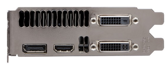
The TDP of the GeForce GTX 760 is 170 watts, and a pair of 6-pin supplemental power feeds are necessary. Outputs on the GeForce GTX 760 consist of a pair of DVI ports, a mini-DP, and an HDMI output. The GeForce GTX 760 has enough muscle to push multiple displays simultaneously, and as such, it supports NVIDIA's 3D Vision Surround technology, as well other proprietary NVIDA technologies like 3DVision, PhyX, and the like.

