Intel Details Cannonlake's Advanced 10nm FinFET Node, Claims Full Generation Lead Over Rivals
However, if you ask Intel about how it approached the developing technologies at the 10nm node, the company will tell you that it is far ahead of its competitors. In fact, Intel stated at its Technology and Manufacturing Day presentation that its 10nm technology is a full generation ahead of the “other guys.” Intel also claims that it has the highest feature density at 10nm and is leveraging the use of hyper scaling to better ensure that it stays well ahead of competitors like Samsung with regards to performance and costs (which are 30 percent lower than its rivals according to Intel).
And if there were any concerns that Moore’s Law is dead, Intel EVP Stacy Smith is trying to put those ideas to rest as well, stating, “Our cost per transistor is coming down at a slightly faster rate than historical. Moore’s Law is alive and well. We are taking bigger steps. We have a three-year lead over the industry.”
So, how does Intel qualify this lead? Besides the fact that Intel is already on its third-generation 3D FinFET process tech, the company was able to shrink its minimum gate pitch from 70nm to 54nm, going from the 14nm to 10nm process nodes. In addition, the minimum metal pitch has shrunk from 52mm to 36mm. As a result, Intel’s logic transistor density at 10nm is 2.7x higher than its previous generation 14nm process, and another 2x greater than its closest competitors.
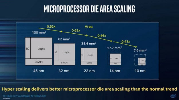
Hyper scaling also allows Intel to improve die area scaling at a faster rate than the usual trends when stepping down to the next node.
As you can see in the chart above, the reductions from 45nm to 32nm to 22nm were a consistent 0.62x, but that scaling stepped up significantly going from 22nm to 14nm and improved yet again going from 14nm to 10nm. This hyper scaling is allowing Intel to produce chips that are either smaller or more densely packed than what its competitors are able to achieve at 10nm.
Intel claims that further refinements at 10nm mean its upcoming Cannonlake processors will provide up to a 25 percent uplift in performance, while consuming 45 percent less power than 14nm counterparts (i.e. Skylake and Kaby Lake). Looking further down the roadmap, Intel has an “enhanced” 10nm process on its roadmap called 10++ that adds another 15 percent performance increase and up to a 30 percent drop in power consumption.
“We are always looking three generations – seven to nine years – ahead,” Smith continued. “Today we have line of sight to 7 and 5 nm. We may not know exactly which approaches will prove best for 5 nm yet, but our culture thrives on those challenges. It has for generations.”


