AMD Radeon RX Vega Unveiled With 8GB HBM2, Up To 27.5 TFLOPs, Starting At $399
The AMD Radeon RX Vega GPU Line-Up

AMD has officially lifted the veil on its new Radeon RX consumer graphics line-up, featuring the company's next-generation Vega GPU architecture. After months of architecture disclosures and rumors, we finally have real specifications and details on the actual Radeon RX Vega graphics card line-up, including pricing, and what AMD is doing to make the cards as attractive as possible for gamers.
Initially, there will be four cards in the Radeon RX Vega line-up, the standard air-cooled Radeon RX Vega 64, a Radeon RX Vega 64 Limited Edition with stylized metal fan shroud, the liquid-cooled Radeon RX Vega 64 Liquid, and the lower-cost Radeon RX Vega 56.
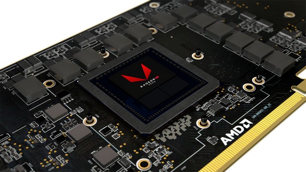
At the heart of all Radeon RX Vega series cards is the Vega 10 GPU. Vega 10 is comprised of roughly 12.5 billion transistors and is manufactured using a 14nm FinFET LPP process. The die size is a beefy 486mm2, which makes it somewhat bigger that Hawaii (438mm2), but smaller than Fiji (596mm2). AMD disclosed that there is over 45MB of SRAM across the chip, and everything is linked its custom serial Infinity Fabric.
The Vega 10 GPU features 4 Asynchronous Compute units, with 4 next-gen Geometry units, and 64 next-gen compute units in its full implementation, with a grand total of 4096 stream processors. There are also 256 texture units on the chip, with 64 render back-ends, which are linked to 4MB of L2 cache. This is double the amount of L2 of Fiji and reduces external bandwidth requirements because there are more cache hits within the larger cache. Vega 10 leverages HBM2 memory for its HBC – or High Bandwidth Cache – connected via a 2048-bit interface.
AMD claims they have made extensive changes to Vega’s design to improve timings across the ASIC. The physical layout of the New Compute Units was optimized with shorter wire lengths for performance-critical paths. The Main ALU maintains its four-stage depth and a maximum of three NCUs (Next-Gen Compute Units) share instruction and constant caches. Due to the design changes, Vega 10 can reliable reach the 1.7GHz range, whereas Fiji hovered around 1GHz and Polaris around 1.3GHz. AMD also mentioned that Vega’s general purpose registers leverage Zen’s custom SRAM design, which results in lower latency than previous architectures, in addition to an 18 percent savings on die area and 43 percent reduction in power.
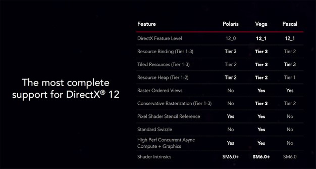
All of the architectural changes, enhancements, and feature additions made to Vega had resulted in the most complete support for DirectX 12 as well.
AMD Radeon RX Vega Product Line-Up
As you’ve probably surmised by this point, the Radeon RX Vega 64’s branding stems from the number of active compute units in its GPU. There are 64 active CUs in a Radeon RX Vega 64 with all 4096 Stream Processors exposed.The base GPU clock speed of the air-cooled Vega 64 is 1,247MHz with a boost clock of 1,546MHz. There is 8GB of HBM2 memory, a.k.a. the High Bandwidth Cache (HBC), on-board that offers up a peak of 484GB/s. All told, the Radeon RX Vega 64 is capable of 12.66 TFLOPs (single-precision) or 25.3 TFLOPs (half-precision) of compute performance.
The frequencies on the liquid-cooled card are somewhat higher. The Radeon RX Vega 64 Liquid-Cooled Edition has the same GPU configuration, but with higher base and boost clocks – 1,406MHz and 1,677MHz, respectively. At those higher clocks, the Radeon RX Vega 64 Liquid-Cooled Edition has peak single-precision compute performance of 13.7 TFLOPs, with 27.5 TFLOPs at half-precision.
The Radeon RX Vega 56 features the same Vega 10 GPU, but 8 of its CUs have been disabled and its clocks are somewhat lower. Radeon RX Vega 56 features 3,584 active stream processors and has a base clock of 1,156MHz and a boost clock of 1,471MHz. At those clocks, the card is capable of 10.5 / 21 TFLOPs of single-precision / half-precision compute performance.
Which brings us to board power. Although AMD has touted a number of efficiency improvements, the Vega RX series requires some serious power. The Vega 56’s board power is in the 210W range, while the top-end liquid-cooled card lands in the 345W range. It remains to be seem what that kind of power means to thermals and acoustics, but rest assured we’ll find out soon enough.
We should also mention that there are two version of the air-cooled Vega 64 coming down the pipeline. There’s a standard version with a cooler that’s reminiscent of the reference Radeon RX 480 and a limited edition card with the all-metal, brushed aluminum shroud. Other features of the cards include an illuminated Radeon logo and “R” pixel at the corner of the fan shroud. Cooling the GPUs on the air-cooled editions is an Isothermic Vapor Chamber linked to a dense array of thin-fins, which is outfitted with a 30mm barrel-type fan.
Update: 7/31/2017 12:13AM There will be more details available later this evening, but AMD also announced the Radeon Pro WX 9100 at $2199 and Radeon Pro SSG, also based on Vega, at $6,999. Both of these professional cards offer 12.3 TFLOPs of FP32 compute performance, 16GB of HBC memory with ECC, and support for up to 6 4K displays @ 60Hz. The Radeon Pro SSG also features 2TB of integrated NVMe Flash storage, linked directly to the GPU for handling massive datasets. The flash storage offers 8GB/s reads, with 6GB/s writes and helps enable things like full 8K editing in real time. We’ll update this section when AMD reveals the full specifications and pricing at is Capsaicin event tonight.


