AMD FX-8150 8-Core CPU Review: Bulldozer Is Here
The Bulldozer Architecture
As we mentioned on the previous page, we won’t be rehashing many of the low-level technical details of AMD’s Bulldozer microarchitecture here, since we’ve already covered them in previous articles. We will, however, cover more product specific details and offer up a condensed refresher of some of the details presented in our previous Bulldozer-related coverage.
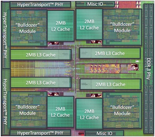
AMD FX-Series Processor Die Map
What you see here is a die map of an AMD FX-Series, 8-core die, formerly codenamed “Zambezi”. It is comprised of roughly 2 billion transistors, is approximately 315mm2, and is manufactured using Global Foundries’ 32nm DSL SOI (silicon-on-insulator) technology. At 315mm2, the Zambezi core used in the FX is somewhat than Thuban's (Phenom II X6) 346mm2, which is good for AMD, but it's still much larger than Sandy Bridge's approximate 216mm2. There is 128 KB of L1 Data Cache (16KB per core), 256 KB of L1 Instruction Cache (64KB per module), and 8MB of L2 Cache (2MB per module), along with 8MB of shared L3 cache. There are four 16-bit HyperTransport links present, although only one is enabled on desktop Bulldozer processors, the others are present for server-class products which are based on the same core design. There is also an Integrated memory controller / northbridge which features two, 72-bit wide DDR3 memory channels.
AMD refers to Bulldozer’s design as a third-way between symmetric multithreading (SMT) like Intel’s Hyper-Threading and true multi-core processing, where multiple discrete cores reside on one die. With Bulldozer, AMD started with two discrete cores, and eliminated some duplicate logic that may have gone unused with the vast majority of workloads. AMD then fused the resulting, pared down cores together into a single, shared design. As far as design efficiency was concerned, taking this route was fruitful as Bulldozer's second ALU unit increased the die size by only 12%. AMD has also emphasized the point that Bulldozer has been architected to be power-efficient. The design features extensive clock-gating throughout, numerous circuits that can be power-gated dynamically, and multiple power-saving features that are under software control (C6 State, Core P-states / AMD Turbo Core, APM, DRAM power management, low power idle state, and C1E).
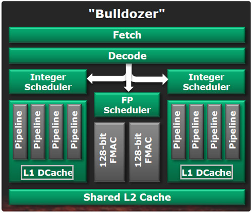
AMD Bulldozer "Two-Core" Module
With Bulldozer, AMD has taken the concept of SMT and essentially added a second independent integer unit. Intel's Hyper-Threading technology improves core efficiency by scheduling multiple threads for simultaneous execution. In a situation where the processor is waiting for code from Thread A, the scheduler can send work for Thread B. This keeps the processor's execution units more fully utilized for longer periods of time, but Hyper-Threading doesn't provide the CPU with any additional execution resources. According to AMD, the company aggressively researched which core blocks needed to be duplicated and which could be combined before finalizing the design of Bulldozer. As far as the OS is concerned, however, each Bulldozer module will appear as a dual-core processor, just as an Intel Hyper-Threaded processor is shown to have double the actual number of actual physical cores.
We should also point out that Bulldozer has four x86 decoders, whereas previous AMD products had just three. And Bulldozer's branch predication units have been optimized for for high performance as well. In fact, branch prediction and instruction fetch logic has been decoupled, which means that an incorrect branch prediction won't stall the fetch unit (and vice versa). Phenom doesn’t have this ability, because the two units are tied to each other.
Bulldozer’s joint FPU unit is capable of tracking two hardware threads (one from each core) and has two MMX integer units and two 128-bit FMAC units. Bulldozer also adds support for SSE4.1, SSE4.2, AVX, AES, in addition to FMA4 and XOP extensions, though software will have to be specifically coded to leverage these resources.

AMD is positioning the FX series at the top of its desktop processor line-up. The E-Series Accelerated Processing Units (APU) are designed for low-power, small form factor, and mobile applications. AMD A-Series APUs are designed for mobile and mainstream desktop applications. And the FX Series is designed for performance-minded consumers and enthusiasts. The feature breakdown above explains what type of workloads each APU / CPU series targets, but it should be noted that there’s nothing stopping a user from plunking a discrete Radeon graphics card into an E- or A-Series APU based system and taking advantage of AMD Eyefinity technology.


