NVIDIA GeForce GTX 680 Review: Kepler Debuts
Kepler Architecture and the GK104 GPU
As we’ve mentioned, the GK104 GPU powering the GeForce GTX 680 is based on NVIDIA’s new Kepler architecture. Kepler, however, is not a complete redesign from the ground up. Although much more power efficient and higher performing than Fermi using a number of key metrics, Kepler does borrow heavily from Fermi’s design.
;)
NVIDIA GK104 GPU Block Diagram
The high-level block diagram above shows the overall structure on the GK104. The chip has an arrangement of four Graphics Processing Clusters (GPC), each with two Streaming Multiprocessors, dubbed SMX (a Streaming Multiprocessors in Fermi is called a SM). Within each GPC, there is control logic, plus 192 CUDA cores, for a total of 1536 CUDA cores per GPU. In the previous-gen GTX 580 (Fermi), there were 32 CUDA cores per SM, which were duplicated 16 times within the chip. With the GK104, there are 192 CUDA cores per SMX, which are duplicated 8 times. The structure results in 6x the number of cores per SM(X) and 3x the total number of cores than the GeForce GTX 580.
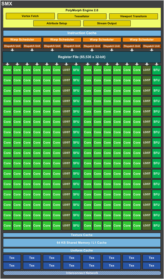
A Close-Up Of A Single SMX In The GK104 GPU
In terms of its other features, the GK104 has a total of 128 texture units and 32 ROPs. There is 512K of L2 cache on-die, and the GPU interfaces with the GeForce GTX 680’s 2GB of GDDR5 memory over a 256-bit interface. It supports DirectX 11 (not 11.1) and features a PCI Express 3.0 host interface. There are eight geometry units in the chip (Polymorph Engine 2.0) and four raster units (one per GPC). According to NVIDIA, the Polymorph 2.0 engines offer double the primitive and tessellation performance per SM of Fermi.
In addition to having a different GPC and SM arrangement, with Kepler, NVIDIA also minimized the hardware control logic in the chip to bring the transistor count down and Kepler will also operate with a single clock domain—shaders/CUDA cores are not clocked at 2x the frequency of the rest of the chip.
With the GK104, the sum total of all of these changes is a 3.54 billion transistor chip with a die size of about 294 square mm, which is manufactured using TSMC’s 28nm process node. If you’re keeping track, that’s about 770M fewer transistors than AMD’s Tahiti GPU in the Radeon HD 7900 series and a significantly smaller die size (294mm2 vs 365mm2) as well.


