ATI Radeon HD 4870 X2 - AMD Back On Top
The Underlying Technology

Although the cards look similar and follow a similar design philosophy, the Radeon HD 4870 X2 differs from AMD's previous dual-GPU based Radeon HD 3870 X2 in a number of ways.
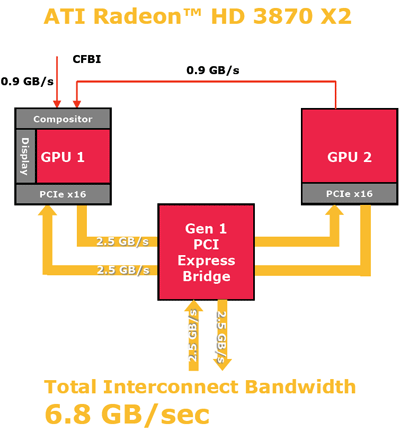
As the above diagram shows, the Radeon HD 3870 X2 featured a pair of GPUs--in its case, RV670s--linked together via a PCI Express gen 1 bridge and a CrossFire bridge interconnect with .9GB/s of peak bandwidth. In total, the design offered an aggregate 6.8GB/s of total interconnect bandwidth across the card.

The Radeon HD 4870 X2 is quite different, however. Of course, the card is built around a new generation of GPUs, namely the RV770. The card is powered by two of the very same GPUs used to power the Radeon HD 4870. They are also linked together by the very same .9GB/s CrossFire bridge interconnect, but the on-board switch used on the Radeon HD 4870 X2 is PCI Express gen 2 based and hence offers twice the bandwidth. Also note that the RV770 GPU features a new sideport interface that offers another 5GB/s of bandwidth between the two GPUs, each way. The combination of a new gen 2 switch and the sideport interface result in a total aggregate interconnect bandwidth on the Radeon HD 4870 X2 of 21.8GB/s, which is more than 3X that of the 3870 X2.
We should note, however, the additional bandwidth afforded by the new sideport is not exploited by current software and applications. Representatives from ATI have informed us that future applications should benefit from the sideport, but they didn't explain exactly how or when. We suspect the sideport may enable AMD to develop new multi-GPU rendering modes, or perhaps enable higher performance in certain stream computing applications. Time will tell.

If you look at the breakdown above, the Radeon HD 4870 X2 isn’t simply two Radeon HD 4870s fused together on a single PCB. The GPUs on the Radeon HD 4870 X2 will be clocked at a minimum of 750MHz and the X2’s gigantic frame buffer memory will be clocked 900MHz (3.6Gpb/s GDDR5 effective), which is similar to the single GPU Radeon HD 4870. But the X2 features double the amount of frame buffer memory, which could help performance at higher resolutions, and it's also outfitted with a gen 2 PCI Express switch.

The Radeon HD 4870 X2's main features and benefits are outlined on the slide above. As you can see, the cards offers up to 2.4 TFLOPS of compute power with its 750MHz core GPU clock and 1600MHz (800 x 2) stream processors. Its 2GB (1024MB per GPU) is clocked at 900MHz, which results in a 3.6Gbps GDDR5 data rate, and total memory bandwidth is 230GB/s (115GB/s x 2). With all that horsepower under the hood, the card has a max board power of 285 watts.
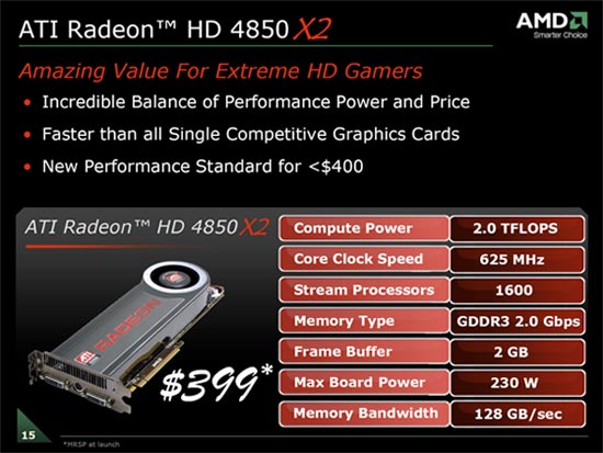
As the old saying goes, "But wait! There's More!" AMD has also informed us that they have a bit of a surprise in the works. A Radeon HD 4850 X2 card that utilizes less expensive GDDR3 RAM is also planned. The Radeon HD 4850 X2's primaary tech specs are outlined in the slide above. With an expected $399 MSRP, the Radeon HD 4850 could wind up being an attractive option in the current 3D graphics landscape and may put even more price pressure on NVIDIA. We hope to have the 4850 X2 in the lab in a few weeks, and will reveal all of its juicy details then. Expected availabilit is sometime in September.


