Logo   Banner   TopRight
TopUnder
Transparent
Intel P35 Bearlake Motherboard And DDR3 Memory – Asus and Corsair
Transparent
Date: May 21, 2007
Section:Motherboards
Author: Dave Altavilla
Transparent
Introduction To Bearlake

Motherboard chipset technology isn't refreshed at the same fevered pitch that processors, memory or IO products are.  A CPU or GPU speed-bump is like low-lying fruit relatively speaking, but chipset enhancements can usher in a whole host of stability, interoperability and verification challenges.  Let's face it, when the product is the basis for a platform foundation, forward migrations can be painful if not carefully planned, so the upside benefits need to be worth-while for both the end customer as well as the manufacturer. 

If you asked us a year ago, what Intel's path to a higher bandwidth system bus and memory access was, we might have told you serial links from the CPU to the Northbridge and serial FBDIMM technology on the system memory.  Of course, that would have been almost completely misguided, since obviously Intel is still pushing hard on their now aging legacy front side bus architecture, with only a hint of a serially connected CPU architecture on the horizon.  In addition, though serial FBDIMMs have taken hold in the server market, where high density memory configurations benefit from the technology's intrinsic signal integrity advantages under multi-drop loads; it won't be showing up in consumer desktop volumes any time soon.

You might say Intel's desktop platform is in transition at this point.  And that transition is being made today to DDR3 memory technology.  The vehicle to get us to the land of higher bandwidth bus speeds and memory is Intel's Bearlake chipset family.  Today we'll be looking at the first of three flavors of Bearlake, the P35 courtesy of Asus, accompanied by Corsair's new XMS3 DDR3 memory modules.  First let's have a quick glance at the entire Bearlake clan. 

blockdiag.png

g33.png

In the mainstream, Intel's new "965" equivalent is the P35.  As you can see, support for DDR3-1066MHz is in there, as well as support for up to a 1333MHz system bus.  You can be sure motherboard manufacturers, like Asus, will offer BIOS options for DDR3-1333 memory speeds as well, though technically the chipset doesn't officially support it.  The chipset does also offer legacy DDR2 memory support, though that will depend on the DIMM sockets that are populated on the board.

chipset.jpg

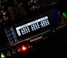
On the subject of memory, Intel has made great strides with the memory controller architecture on the Bearlake family of chipsets.  Dubbed "Fast Memory Access" technology (talk about vaugue!), Intel has also tweaked and optimized latency characteristics of the Memory Controller Hub (MCH).  That, coupled with the latency enhancing 8-bit prefetch of DDR3 (versus 4-bit -prefetch in DDR2), and the pair should prove to be a potent combination.

Beyond that, we see that Intel has revamped their ICH Southbridge technology, now known as ICH9R.  The new Southbridge has support for a total of 6 SATA ports, with Intel Matrix Storage RAID technology and Intel "Turbo Memory" support for Microsoft's Vista ReadyBoost flash-based hard disk caching.  On a side note, Intel has added another pair of USB ports to the Southbridge as well, increasing that capacity up to 12 total. 

Finally, the G33 chipset will be essentially a P35 equivalent, but with the added benefit of Intel's integrated Graphics Media Accelerator 3100 with "Clear Video" technology.  Though we haven't yet put Clear Video to the test, in this incarnation of the chipset, consider the technology similar to what is offered in Intel's G965 chipset, for hardware assist of high definition video processing, motion compensation and other IQ enhancements.

Transparent
The X38 And G35 Chipsets

Below we have a quick-take of Intel's 12 month chipset roadmap.  Here we see where each variant is to be positioned in the desktop market, both mainstream and high-end.

roadmap.png

Notable data-points on this slide are the future G35, X38 and Eaglelake family of chipsets.  The X38 specifically will usher in PCI Express 2.0 serial technology with its bi-directional 5Gb/s SerDes (serializer/de-serializer) technology, essentially doubling available bandwidth over PCI Express 1.0a  and 1.1 standards-based products.  These 32 PCI Express 2.0 lanes, will also be backwards compatible, auto-negotiating down to PCI Express 1.1 data-rates as needed.  When this chipset hits the market, it is bound to be potent.  Beyond the X38, Eaglelake, slated for sometime in Q2'08, will bring forth Intel's ICH10 Southbridge and support for HD-DVD/Blu-Ray processing, among other enhancements.

  x38.png 

g35.png

Much like the dynamic duo of the P35 and G33, the X38 chipset will have an integrated graphics empowered counterpart, namely G35.  G35 will mark Intel's first DX10 compliant graphics core, with full support for SM4.0 rendering.  Note the emblazoned Windows Vista logo of course, which will be prominent branding we are sure, on the retail shelves and case badge artwork.  The G35 will also have support for HDCP over what Intel calls "SDVO" or Intel's Serial Digital Video Out technology.  SVDO is an Intel proprietary mechanism for transfering digital display CODEC functions over the PCI Express interface.  The technology has actually been around since the 945G series chipset was introduced.

Transparent
Asus P5K3 Deluxe P35 Motherboard And Corsair DDR3

All this technology, at the chip level, might be interesting but to many of you, we're sure the final product has even more appeal.  In the pages ahead, we'll provide performance data take from a new Asus P35 motherboard, dubbed the P5K3 Deluxe WiFi Edition.  We also have a set of test metrics for comparison, taken on a variant of the board that is built to support legacy DDR2 memory.  First let's look at one of the first motherboards on the market built to support DDR3 memory technology.

small_p5k3_deluxe.jpg
Asus P5K3 Deluxe WiFi Edition

Asus P5K3 Deluxe 
Asus P35, DDR3 Ready 

CPUs Supported
- Core 2 Extreme / Core 2 Duo / Core 2 Quad
- Pentium Extreme / Pentium D / Pentium 4
Chipset:   P35 / ICH9R with Intel Fast Memory Access
System Bus:  1333 / 1066 / 800MHz
Memory:   4 x DIMM, max 8GB, DDR3 1333/1066/800MHz
Expansion Slots:   2 x PCI-E X16 (one X16 and one X4/X1 mode), 2xPCI-E X1, 3xPCI 2.2
Storage/Southbridge:   6 x SATA 3.0Gb/s ports, Intel Matrix RAID 0,1,5,10
Storage/JMicron:   1xUDMA133, 2xExternal SATA 3.0Gb/s - RAID 0,1
LAN:   Dual Gigabit LAN - Marvell 88E8056 PCI-E, Realtek RTL8187 PCI
Wireless LAN:  Asus WiFi-AP Solo - 54Mbps IEE802.11g
Audio:    ADI AD1988B 8-channel High Definition Audio CODEC
USB:   10 x USB 2.0, 4 ports internal, 6 ports IO back panel
Firewire:   Agere FW322 1394a, 2 x IEEE 1394a, 1 internal, 1 back panel
 

small_p5k3_kit.jpg   small_ports.jpg  small_pipes.jpg

small_socketram.jpg   small_south.jpg  small_slots.jpg

The P5K3 Deluxe is decked out in typical Asus flare.  Copper heat-pipes surround its socket area, providing passive cooling supported by optional clip-on turbine fans, for its Northbridge and a CPU power array.  The ICH9R Southbridge heatsink is also tapped into the cooling pipe assembly as well.  Asus brought out all six SATA ports from the ICH9R and even added an additional standard PATA port for optical drives, along with two external eSATA ports on the IO back-plate, courtesy of an additional JMicron controller.  Additionally, Asus saw fit to bring out six USB2.0 port on the back panel, a welcomed addition for sure, doing away with an ancient PS2 mouse port.  Also, as its full name suggests, the version of the board we tested came with Asus' integrated 54g WiFi NIC that can also turn your system into a WiFi Access Point.  This is an option on the P5K3 Deluxe series of boards and Asus will offer models without it as well.

In terms of slot configurations, this motherboard comes equipped with a pair of X16 PCI Express slots but don't let that fool you.  The second black colored slot is only enabled with a X4 PCI Express connection.  This is due to the fact that the P35 chipset only has 22 lanes of PCI Expres connectivity.  We will take one small issue with the PCB layout approach Asus took with this motherboard.  Move that clear CMOS jumper out from under the first PEG slot area, please.  Having to pull a graphics card to hard reset the CMOS is simply a drag.

Other than that small sniggle, the board really flies and is heavily geared to the tweaker and overclocker.  Since this is more of a platform showcase than anything else, we don't have our usual array of BIOS screen shots.  However, suffice it to say that you can tweak bus and memory speeds, latency settings, voltages, etc, to your hearts content and with lots of stability.  We'll get to our own overclocking efforts and results later on.

Transparent
Corsair XMS3 DDR3 Memory

It seems like only yesterday we were poking and prodding at DDR2 memory in an effort to see what new-found performance levels we could achieve.  If you recall, in its introductory stages, DDR2 exhibited marginal performance benefits over standard DDR memory, mainly due to its higher latency characteristics in timing and access.  DDR3 will go through much the same development and bring-up cycle.

Corsair XMS3 DHX - CM3X1024-1333C9DHX - DDR3 DRAM
Early DDR3 Engineering Samples But Promising
  • 667MHz Double Data Rate
    • CL 9-9-9-24 Timings
  • 533MHz Double Data Rate
    • CL 7-7-7-21 Timings
  • 240 pin notched DIMM
  • 1.5V supply voltage
  • 8-bit Prefetch
  • On-Die Termination

small_corsair.jpg     small_corsairfins.jpg

Though all our tests were performed with Corsairs XMS3 CM3X1024-1333C9DHX modules, we also plugged in a pair of CM3X1024-1066C7 modules as well.  Ultimately the Dominator DHX (Dual Path Heat eXchange) sticks you see here offered the best overall performance.  While both sets of DIMMs could handle 1333MHz performance, neither could get below CAS8 timings.  The DHX variety we tested hit CL 8-6-6-15 timings at 1333MHz, which was about as fast as we could go at any voltage.  Incidentally, 1.9V definitely seems to be the sweet spot in terms of overclocking and top-end performance.  More on that subject, later.

Everest  Testing DDR3 Vs. DDR2
Bandwidth And Latency Measurements

We first set out to quickly analyze this new type of memory with Lavalys' EVEREST Cache and Memory Benchmark.  Certain aspects of chipset timings were reporting incorrectly but this didn't affect the performance measurements.

small_everest_ddr3_1333cl8.png
DDR3-1333 CL8,6,6,15

small_everest_ddr3_1066cl7.png
DDR3-1066 CL7,6,6,15

small_everest_ddr2_1066cl5.png
DDR2-1066 CL5,5,5,15

As you can see, we're running a standard Core 2 Duo E6700 chip beyond its rated bus speed at 333MHz for a quad-pumped 1333MHz total FSB speed and 1333MHz DDR3 memory speed.  We then kept the same bus speed but dropped the memory speed down to 1066MHz CL6 and later ran the DDR2 version of the P5K3 motherboard we had, with standard DDR2 memory at 1066MHz CL5.  As you can see, DDR3 at 1333MHz offers the best combination of both raw read/write/copy throughput and latency.  Read bandwidth was on the order of about 7% higher than standard DDR2 on the same chipset (P35) and our latency numbers were shaved down by about 2ns at these speeds, though timings for the DDR3-1333MHz setting were pokey at 8,6,6,15.  Frankly, there is no question this new platform offers measurable gains in performance due in part to the faster memory controller on the P35 chipset, but the high latency characteristics of current DDR3 memory are holding things back quite a bit, as was the case with DDR2 at its inception.  In the months ahead, hopefully manufacturers like Corsair can get timings down closer to CL5 or 6 at 1333MHz.

Transparent
Test System Setup And SiSoft SANDRA CPU

Below are our test system configurations for a proper perspective of how we tested.  For our processor, we chose a 2.66GHz Core 2 Duo E6700 chip, that when setup with a 333MHz FSB and multiplier of 9X, also runs at an even 3GHz at stock voltage.  At this setting we obtained a 1333MHz FSB and matching 1333MHz DDR3 speed.  1066MHz FSB speeds were recorded at the processor's stock setting of 266MHz with a multiplier of 10X.

HotHardware's Test Systems
AMD & Intel Inside!

System 1:
Intel Core 2 Duo E6700 (2.66GHz And 3GHz)

Asus P5K3 Deluxe WiFi Ed. 
(Intel P35 Bearlake Chipset)

Asus P5K Deluxe (DDR2)
(Intel P35 Bearlake Chipset)

2x1024MB Corsair PC2-8500
CL 5-5-5-15-2T - DDR2-1066

2x1024MB Corsair XMS3
CL 8-6-6-15-2T - DDR3-1333
CL 7-6-6-15-2T - DDR3-1066

GeForce 8800 GTX
On-Board Ethernet
On-board Audio

WD740 "Raptor" HD
10,000 RPM SATA

Windows XP Pro SP2
NVIDIA Forceware v158.22
DirectX 9.0c

System 2:
Intel Core 2 Duo E6700
(2.66GHz)

Asus P5B Deluxe WiFi Ed.
(Intel P965 Chipset)

2x1024MB Corsair PC-8500
CL 5-5-5-15-2T - DDR2-1066

GeForce 8800 GTX
On-Board Ethernet
On-board Audio

WD740 "Raptor" HD
10,000 RPM SATA


Windows XP Pro SP2
NVIDIA Forceware v158.22
DirectX 9.0c

   
Preliminary Testing with SiSoft SANDRA XI SP2
 Synthetic Benchmarks

We began our testing with SiSoftware's SANDRA, the System ANalyzer, Diagnostic and Reporting Assistant. We ran three of the built-in subsystem tests that partially comprise the SANDRA XI suite (CPU, Memory Bandwidth, and Latency) with the a Core 2 Duo E6700 at 2.66GHz and overclocked with a 333MHz FSB and 9X multiplier at 3GHz.


In these tests, we learn that Front Side Bus speed really doesn't equate to any advantage in compute throughput.  However, looking at the second set of Whetstone iSSE3 scores, we see the apparent advantages of Intel's new Bearlake chipset and possibly the influence of the new MCH.  At identical settings, with a 1066MHz FSB and a 2.66GHz CPU clock, the P35-based Asus motherboard outpaced the P965-based system by about 3%.

Transparent
SiSoft SANDRA Memory Bandwidth And Latency

The following SANDRA Memory Bandwidth tests should allow us to home in on performance levels at various bus and memory speeds as well as latency timings with our new DDR3 memory.

 SiSoft SANDRA XI SP2 - Memory Bandwidth And Latency
 Synthetic Benchmarks


In terms of overall bandwidth, a combination of a 1333MHz front side bus, coupled with 1333MHz DDR3 memory, offered the best overall performance.  Clearly the higher latency settings of DDR3 are curbing throughput however, as is obvious in our 1066MHz tests, where 1066MHz DDR2 memory at CL5 obviously edged out DDR3-1066 at CL7.  Interestingly, this was not the case in our 1066MHz memory tests with a 1333MHz FSB.

The latency picture told the story most dramatically of all perhaps.  The combination of a synchronous 1333MHz FSB and 1333MHz memory interface produced latency characteristics some 7% faster than the P965/DDR2 chipset and memory combination. However, if you don't have your clock speeds up, DDR3's current latency shortcomings will bite you in the backside.

Transparent
PCMark CPU And Memory Testing

For our next round of synthetic benchmarks, we ran the CPU and memory performance modules built into Futuremark's PCMark05 suite. 

Futuremark PCMark05
More Synthetic CPU and Memory Benchmarks

"The CPU test suite is a collection of tests that are run to isolate the performance of the CPU. The CPU Test Suite also includes multithreading: two of the test scenarios are run multithreaded; the other including two simultaneous tests and the other running four tests simultaneously. The remaining six tests are run single threaded. Operations include, File Compression/Decompression, Encryption/Decryption, Image Decompression, and Audio Compression" - Courtesy FutureMark Corp.


There really isn't much of a story to tell here.  Perhaps it's time to finally retire PCMark05 from our test suite.  The CPU performance module shows a keen sense of the obvious.  Like processor clock speeds equate to similar performance metrics.


"The Memory test suite is a collection of tests that isolate the performance of the memory subsystem. The memory subsystem consists of various devices on the PC. This includes the main memory, the CPU internal cache (known as the L1 cache) and the external cache (known as the L2 cache). As it is difficult to find applications that only stress the memory, we explicitly developed a set of tests geared for this purpose. The tests are written in C++ and assembly. They include: Reading data blocks from memory, Writing data blocks to memory performing copy operations on data blocks, random access to data items and latency testing."  - Courtesy FutureMark Corp.


Our PCMark memory performance tests at least correlated with what we saw in our SANDRA bandwidth, though the spread in the field was much tighter.  A smallish 2% advantage is afforded to the Asus built P35 motherboard and Corsair DDR3 memory at 1333MHz, versus DDR2 memory on the same chipset.  Additionally, PCMark doesn't show the P35 chipset with much of a lead over the P965 at like speeds and memory configurations.

Transparent
HD Tach ICH9R Vs. ICH8R HDD Subsystem Performance

In our next series of tests, we wanted to observe the performance characteristics of Intel's new ICH9R Southbridge and its SATA controller implementation.  We hooked up a blank Western Digital Raptor WD1500 10K RPM drive to a SATA port on both the Asus P5K3 motherboard with its ICH9 Southbridge and our 965 board with its ICH8R Southbridge.  Though this was a quick and dirty single drive test, we'll be looking at RAID performance, in various configurations, in the weeks and months ahead.

HD Tach Storage Subsystem Benchmark
Long Test With Writes On WD Raptor WD1500 Drive 


Intel clearly has refined their SATA controller design in the ICH9R.  A consistently observable 2 - 4% advantage was shown across the board in all measurements, burst, average read and average write. Though these aren't huge gains, any gain is simply goodness.

Transparent
Office XP And Photoshop Performance

PC World Magazine's Worldbench 5.0 is a Business and Professional application benchmark.  The tests consist of a number of performance modules that each utilize one, or a group of popular applications to gauge performance. 

Worldbench 5.0: Office XP SP2 and Photoshop 7 Modules
Real-World Application Performance

Below we have the results from WB 5.0's Office XP SP2 and Photoshop 7 performance modules, recorded in seconds.  Lower times indicate better performance here, so the shorter the bar the better.


Worldbench's Office XP SP2 performance module had the new Asus P35-based motherboards finishing this test slightly faster than the P965 when operating at a 1066MHz FSB, with similarly clocked memory.  And the lower-latency DDR2 equipped P35 nudged ahead of the higher-latency DDR3 setup.  Up the FSB to 1333MHz, and the scores improve across the board, but notice that latency still proves to be the deciding performance factor.

photoshop.png

Our Photoshop test, however, was completely devoid of any meaningful data on the benefits of each system architecture.  Plain and simple, this version of Photoshop is looking for faster CPU cores to do its work, regardless, of system or memory bandwidth.

Transparent
Windows Media Encoder Multitask And 3D StudioMax

Below we have the results from WB 5.0's Windows Media Encoder/Mozilla multitask and 3D Studio Max performance modules, recorded in seconds.  Lower times indicate better performance here, so the shorter the bar the better.

Worldbench 5.0: Windows Media Encoder/Mozilla MT And 3D StudioMax  
Real-World Application Performance

wme9_multitask.png

3dsmax.png

Our multitasking test showed the obvious advantage of both bus speed and memory bandwidth at 3GHz settings.  However, settling down to a 1066MHz bus, the field closes in tightly with no significant advantage to any one system configuration.  3D Studio Max showed a consistent, small edge to the Intel P35-based test machines, as well as higher speed DDR3-1333 memory.

Transparent
3DMark06 CPU Test and Cinebench 95 3D Rendering

The Cinebench 9.5 benchmark is an OpenGL 3D rendering performance test, based on the commercially available Cinema 4D application. Cinema 4D from Maxon is a 3D rendering and animation tool suite used by 3D animation houses and producers like Sony Animation and many others.  And of course it's very demanding of system processor resources.

Cinebench 9.5 Performance Tests
3D Modeling & Rendering Tests

This is a multi-threaded, multi-processor aware benchmark that renders a single 3D scene and tracks the length of the entire process. The time it took each test system to render the entire scene is represented in the graph below (listed in seconds).


Cinebench was sort of a roll of the dice and it didn't particularly favor the P35 chipset at all.  In the end, the multi-threaded scores perhaps show the most meaningful data but oddly, the 965 based system had a slight edge.

Futuremark 3DMark06 - CPU Test
Simulated DirectX Gaming Performance

3DMark06's built-in CPU test is a multi-threaded "gaming related" DirectX metric that's useful for comparing relative performance between similarly equipped systems.  This test consists of two different 3D scenes that are generated with a software renderer that is dependent on the host CPU's performance.  This means that the calculations normally reserved for your 3D accelerator are instead sent to the central processor.  The number of frames generated per second in each test are used to determine the final score.

3dmark_cpu.png

3DMark06's CPU performance module requires the CPU to provide software-base rendering of scenes.  As such, it's heavily geared toward pure processor throughput.  There really wasn't much to report in this test.

Transparent
Quake 4 And Half Life 2 : EP1 Gaming Performance

For our next set of tests, we benchmarked all of the test systems using custom single-player Quake 4 and HL2: EP1 timedemos. Here, with Quake we installed the game's official v1.3 point release which is SMP capable. And we turned the resolution down to 800X600 to take the load off our GeForce 8800 GTX cards.  Although Quake 4 typically taxes today's high-end GPUs, when it's configured at these minimal settings, it is much more CPU and memory bandwidth-bound than anything else. For the EP1 testing, we performed a siimlar procedure, with the game set to 800X600 with HDR disabled.

CPU Benchmarks with Quake 4 And Half Life 2 : EP1
Gaming Performance

q4.png

Comparing notes, there's roughly a 3% advantage for our Bearlake-based systems, versus the P965 chipset-based system.  The other take-away is that at 1333 FSB and 3GHz CPU speed, memory bandwidth or latency didn't matter much, it's all about CPU clock speed with Quake.

ep1.png

Half Life 2, on the other hand, does show a tendency toward memory bandwidth, as you can see ever so slightly in the 3GHz DDR3-1333 enabled score.  Other than that, no significant marginalities are observed.

Transparent
Fun With Overclocking DDR3

Before we called it a day, we decided to see what this new memory from Corsair could really do.  We turned up latency timings a bit and cranked our FSB and BIOS divisors to push our DDR3 modules as high as they could go.  Here are the results...

Overclocking Corsair DDR3 Memory
1700MHz+ DDR Memory Speeds

small_cpuz_oc1733.png   small_cpuz_oc1733_timings.png
System Bus Speed And DDR3 @ 1730MHz
CL 10,8,8,16

True, CAS10 timings do cause you to wince in pain a bit but look at that clock speed.  1.73GHz is no small feat for DRAM memory technology.  We're looking forward to days when perhaps we could hit this speed at CL8?  Do we hear CL7?  Time will tell.

small_san_bigoc1733.png   small_everest_oc1733.png
SANDRA And Everest Memory Bandwidth Performance

We've actually recorded similar memory bandwidth scores in SANDRA with DDR2 memory at 1100MHz+ and an FSB this high but regardless, it's promising to see a 1700MHz data-rate.  We gained about 6% more read bandwidth in this configuration.  However, we chalked up a 30% increase in write bandwidth, according to EVEREST, nothing to sneeze at and it correlates directly to the 30% increase in clock speed.

Transparent
HotHardware Conclusion

Performance Summary:
Over the course of our testing, we saw the new Intel P35 chipset and DDR3 memory combination offer up gains in the 2 - 5% range in various applications.  This was largely attributed to the new Intel MCH and its improved access latency characteristics.  There were several occasions where the P35 chipset driven Asus P5K3 Deluxe out-paced its 965 counterpart with the same DDR2 memory running in its DIMM slots.  In terms of DDR3 memory, it's obvious the technology is still maturing somewhat but at its higher clock speeds, especially with a correspondingly higher FSB, there are significant gains to be had. 


Intel's new Bearlake chipset family is off to a great start with the P35.  Our first time out with this new chipset showed surprisingly good stability and performance with obvious headroom for growth. One look at a 1733MHz DDR3 clock speed and you can't help but get a little bit excited for what the future holds.  The only caveat will be how quickly latency settings can be brought in line.

At this point in the game, if you were building a new system for work or pleasure, its probably doesn't make sense to spring for a DDR2 driven version of one of these new P35 motherboards, like the Asus P5K we tested.  The product simply will have a more finite life-span with the inevitable migration to DDR3.  In addition, DDR3 has a bit of growing-up to do for the next few months, so we'd recommend users wait and see what second generation products coming down the pipe will offer perhaps.  Refinements in motherboard design are bound to be forthcoming, as well as tighter timings for DDR3.

Though, if you're itching for something to tinker with and spending a little extra cash on being an early adopter isn't out of the norm for you, we'd say jump in, the water is just fine.  The P35 chipset with its snappy new memory controller impressed us more-so than many chipset product launches of late and we've seen plenty.  What's perhaps more exciting is the upcoming X38 chipset with PCI Express 2.0 technology and a few extra lanes integrated with the chipset to boot.  It's always hard to judge the entry point with a new platform but these are good problems to have.


  • Faster MCH Memory Controller
  • DDR3 1333 - 1700MHz
  • Faster ICH9R Southbridge
  • Lower Power
  • 1333MHz FSB    
  • High Latency DDR3
  • Pricey for early adopters  

Discuss This Article In HotHardware's PC Hardware Forum...

Or Read The News Release And Comment On HH Live 


Content Property of HotHardware.com