Intel and Micron Unveil 25nm NAND Flash
25nm NAND Is Here

IM Flash Technologies is a joint venture between Intel and Micron that is targeted for producing NAND flash memory. With a focus on research and development, IMFT has doubled NAND density approximately every 18 months. In 2006, they started production with a 50nm process, then moved to a 40nm process in 2008. This co-development inevitably lead to smaller, more affordable NAND flash-based products featuring higher capacities, much like we have witnessed in the SSD market and with USB flash drives over the past couple of years. February 1, 2010 will mark the official announcement of IMFT's 25 nanometer NAND technology--a major advancement for the company. Intel and Micron now lay claim to the smallest production ready semiconductor process technology in the world. The companies describe their collective efforts as such...
“To lead the entire semiconductor industry with the most advanced process technology is a phenomenal feat for Intel and Micron, and we look forward to further pushing the scaling limits,” said Brian Shirley, vice president of Micron’s memory group. “This production technology will enable significant benefits to our customers through higher density media solutions.”
“Through our continued investment in IMFT, we’re delivering leadership technology and manufacturing that enable the most cost-effective and reliable NAND memory,” said Tom Rampone, vice president and general manager, Intel NAND Solutions Group. “This will help speed the adoption of solid-state drive solutions for computing.”
We also have a bit of video from the actual briefing on IMFT's new 25nm technology, as it was being given. In the video above, you can hear Intel VP Tom Rampone and Micron VP Brian Shirley talk about 25nm process technology and its features and benefits.
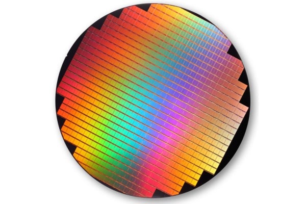
25nm Wafer
So what does this mean for consumers? Basically, the shrink to 25nm reduces the dies size of the NAND flash chips, which enables higher densities, and hence the chip count within products can be reduced by up to 50% when compared to the previous process generation. It allows for smaller, yet higher density designs at lower costs. For example, a particular SSD may be able to be produced using only 16 chips versus 32. Solid State Drives will feature larger maximum capacities while prices of current options will be driven further down. We were told to expect performance to be on par with 34nm products, though there are the obvious intrinsic benefits of a die geometry shrink from a performance standpoint. 8GB MLC NAND Device - 167mm²
Of course, there will be a number of products based on this technology over time. The first one will be the industry's first monolithic 8GB NAND device. At a die size of 167mm², it is twice the capacity of their highest density 34nm part in roughly the same footprint. It is small enough to fit through the hole in the middle of a compact disc, but is able to store more than 10 times the data capacity of a CD. In roughly the same real estate, SSD makers will now be able to provide double the capacity as the previous generation.
 IMFT is on track to begin production of this device and expects to start shipping in the second quarter of this year. Consumers can expect products featuring 25nm flash memory towards the end of 2010.
Micron and Intel are also supporters of the Open NAND Flash Interface (ONFI). ONFI is a consortium of tech companies working to develop open standards for NAND memory and supporting devices. The formation of the group was initially announced at the Intel Developer Forum in 2006 and began the effort to standardize the low level interface to NAND flash chips that are on the market today. One of the main motivations for this is to make it easier to switch between chips from different manufacturers, which allows faster development of NAND-based products and lower prices through broader competition among manufacturers. Besides Intel and Micron, the ONFI consortium is led by several prominent manufactures of NAND such as Hynix, SanDisk, and Sony.
The 8GB NAND device shown above supports the ONFI 2.2 interface standard, delivering up to 200MB/s of throughput bandwidth. Both Intel and Micron have been pleased with it and feel it is very much in tune to what they have driven in the DRAM world, using standard synchronous interfaces to increase speed. This is critical when SSD manufacturers rely on high speed communication between chips.


