AMD Vega GPU Architecture Details Revealed
A Closer Look At AMD's Vega GPU Architecture

Although GPUs based on the technology are not quite ready to ship, AMD recently briefed us on some of the finer details of its next-generation architecture, codenamed Vega.
One of the underlying forces behind Vega’s design is that conventional GPU architectures have not been scaling well for diverse data types. Gaming and graphics workloads have shown steady progress, but today GPUs are used for much more than just graphics, and this fact was at the core of Vega’s design philosophy.
Game install sizes are also expanding exponentially, to the point where they may reach 10’s of gigabytes now. The professional graphics space works with even larger datasets, which may creep into petabyte territory, with some groups even dealing with exabytes of data. Addressing such massive amounts of data presents a major challenge as well.
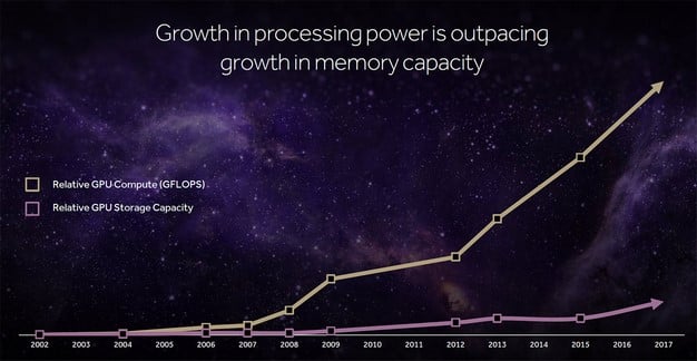
The compute capability of GPUs may have been increasing at a good pace, but memory capacity has not kept up. Vega aims to improve both compute performance and ultimate memory capacity, however, through some new technologies not available on any previous-gen architecture. In fact, AMD claims Vega has over 200 new features, though we can’t quite tell you about all of them just yet.
There were four main points that AMD wanted to drive home in our initial briefings. First, is that Vega has the most scalable GPU memory architecture built to date. It also has a new geometry pipeline, tuned for more performance and better efficiency, a new Compute Unit design, and a revamped pixel engine. All told, Vega should offer significant improvements in terms of performance and efficiency when products based on the architecture begin shipping in a few months.
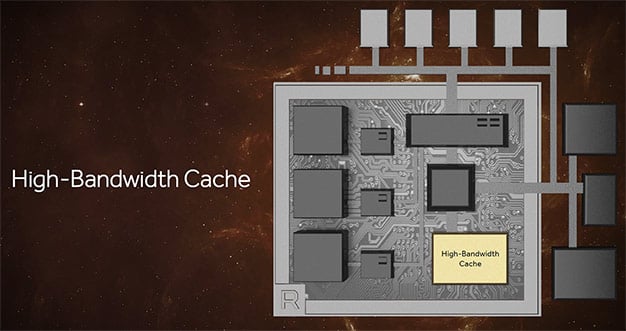
We’ll start our Vega discussion with some information regarding its High Bandwidth Cache. This is essentially the name AMD is giving to the HBM2 -- the second-generation high bandwidth memory -- attached to Vega. Though the HBM2 connected to the GPU does behave like traditional VRAM when necessary, Vega’s memory architecture treats it more like one level in the GPU’s memory hierarchy. All of the HBM2 is available to the GPU, where it’ll be used for the active working data set, but AMD wants Vega to have fast access to all of the available memory in a system. Think of the HBM2 as a portal where the most pertinent data is stored.
While we’re on the subject of HBM2, a quick refresher is probably in order. HBM2 will offer double the bandwidth of HBM1 per pin, at similar clocks. But take note that HBM2 is an evolutionary technology that will scale up even further over time. Like HBM1, HBM2 is also more efficient and has a smaller footprint than other graphics memory types, and has up to 8X the density per stack, to reduce its physical footprint. The 4GB limitation that held AMD’s current HBM1-infused Fury-branded products back will be eliminated with HBM2, though depending on the number of stacks employed on the GPU, peak bandwidth may or may not change much.
AMD has also implemented what it is calling a High Bandwidth Cache Controller in Vega. The HBCC gives the GPU access to 512TB (half a petabyte) of virtual address space and gives the GPU fine-grained control, for adaptable and programmable data movement. Often, more memory is allocated for a particular workload than is necessary; the HBCC will allow the GPU to better manage disparities like this for more efficient use of memory. The huge address space will also allow the GPU to better handle datasets that exceed the size of the GPU’s local cache. AMD showed a dataset being rendered in real-time on Vega using its ProRender technology, consisting of hundreds of gigabytes of data. Each frame with this dataset takes hours to render on a CPU, but Vega handled it in real-time.


