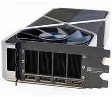
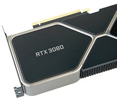
NVIDIA GeForce GTX 285 Unveiled
Introduction and Specifications

One short week ago, NVIDIA unveiled the GeForce GTX 295, and with it reclaimed the overall 3D performance crown from a resurgent AMD. As you may know by now, the dual-GPU powered GeForce GTX 295 features a pair of re-worked GT200 GPUs, manufactured using a more advanced 55nm fabrication process than its 65nm predecessor. Looking at the specifications for the individual GPUs used on the GeForce GTX 295, however, revealed something interesting. You see, the GPUs on the GeForce GTX 295 featured a full complement of 240 shader cores, like the former flagship GTX 280, but they had "only" a 448-bit memory interface. The GeForce GTX 280 had a 512-bit interface.
NVIDIA didn't simply lop off a memory partition to create the GPUs for the GTX 295 though. The 55nm GT200B GPUs are fully capable of utilizing a 512-bit interface. NVIDIA chose to implement a 448-bit memory interface per GPU on the GTX 295 to decrease board complexity, and quite frankly because they didn't need to go any wider to have the fastest graphics card on the market. But that meant the GT200B GPU, as it's implemented on the GTX 295, wasn't being used to its fullest potential. This changes today.
Although the GeForce GTX 285 we'll be showing you here hasn't exactly been a well kept secret, its final specifications and performance have been. As its name implies, the GeForce GTX 285 is a step up from the GTX 280. Just how large of a step up remains to be seen, however. Hopefully, we'll be able to find out in the pages ahead as we take the GeForce GTX 285 for a spin through a complete battery of benchmarks, including some numbers from the just-released hot new game title, Mirror's Edge.

NVIDIA GeForce GTX 285
|
|
|
|
Fabrication Process |
55 nm |
|
Core Clock (texture and ROP units) |
648 MHz |
|
Shader Clock (Stream Processors) |
1476 MHz |
|
Memory Clock (Clock rate / Data rate) |
1242 MHz / 2484 MHz |
|
Total Video Memory |
1 GB |
|
Memory Interface |
512-bits |
|
Total Memory Bandwidth |
159.0 GB/s |
|
Processor Cores |
240 |
|
ROP Units |
32 |
|
Texture Filtering Units |
80 |
|
Texture Filtering Rate |
51.8 GigaTexels/sec |
|
Connectors |
2 x Dual-Link DVI-I 1 x 7-pin HDTV Out |
|
RAMDACs |
400 MHz |
|
Bus Technology |
PCI Express 2.0 |
|
Form Factor |
Dual Slot |
|
Power Connectors |
2 x 6-pin |
|
Max Board Power (TDP) |
183 watts |
|
GPU Thermal Threshold |
105° C |
The core GPU technology employed in the GeForce GTX 285, is essentially identical to the GeForce GTX 280, save for the fact that the GT200B GPU used on the 285 is manufactured at 55nm. As such, we won't rehash the same information we've covered in the past in this article. If, however, you'd like to learn more about what the GT200, and GT200B by extension, are made of, be sure to check out our coverage of the original GeForce GTX 280 and GTX 260 launch from June of last year. While you're at it, our coverage of the recently released GeForce GTX 295 is available right here. Reading those two articles will lay all of the foundation necessary to understand what's processing the pixels under the GeForce GTX 285's virtual hood.
As you can see in the list above, the GeForce GTX 285's reference specifications call for a 648MHz core clock and a 1476MHz shader clock, with 1GB of GDDR3 memory running at 1242MHz (2484MHz DDR). The card sports a 512-bit memory interface and at the clocks mentioned here, it offers total memory bandwidth of 159GB/s. The number of shader cores (240), ROP units (32), and texture filtering units (80), remains unchanged from the GeForce GTX 280. Max board power has been reduced to 183 watts, from 236 watts on the 280. And the card needs only a pair of 6-pin PCI Express power feeds. No 8-pin feeds are necessary.


