Intel Skylake Gen9 Series Graphics Architecture Unveiled
Straight to the point, the Core i7-6700K is Intel's fastest quad-core desktop processor to date. However, one thing we didn't go too in-depth with is the integrated graphics, and that's because Intel kept a tight lid on the underlying technology. That is, until now.
Lo and behold, there's a whitepaper on Intel's website detailing the compute architecture of Intel's "Gen9" graphics. It's an update to the Gen8 whitepaper, though specific architecture changes to Gen9 are noted throughout.
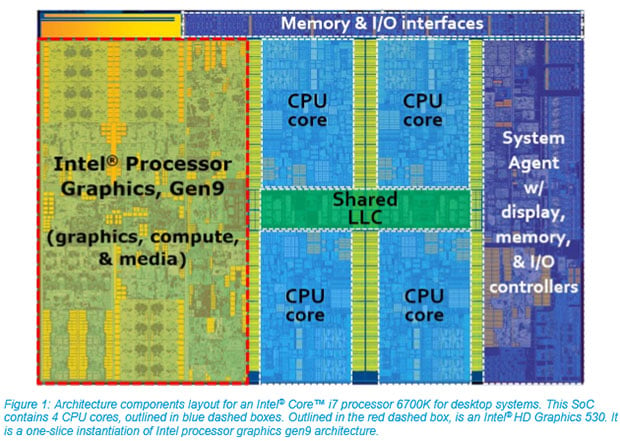
As with previous Core processors, Skylake uses a System-on-Chip (SoC) architecture, a term you hear fairly often in the mobile world with regards to chips like Qualcomm's Snapdragon series and Apple's custom A-series. Specific to the 6700K are four CPU cores, Intel HD Graphics 530, shared LLC, memory and I/O interfaces, and various controllers, as shown above.
"Intel 6th generation Core processors are complex SoCs integrating multiple CPU cores, Intel processor graphics, and potentially other fixed functions all on a single shared silicon die," Intel explains. "The architecture implements multiple unique clock domains, which have been partitioned as a per-CPU core clock domain, a processor graphics clock domain, and a ring interconnect clock domain. The SoC architecture is designed to be extensible for a range of products, and yet still enable efficient wire routing between components within the SoC."

None of this is really new, so what makes Gen9 special? Here's an overview of the changes Intel made specific to Gen9.
Gen9 Memory Hierarchy Refinements
- Coherent SVM write performance is significantly improved via new LLC cache management policies.
- The available L3 cache capacity has been increased to 768 Kbytes per slice (512 Kbytes for application data).
- The sizes of both L3 and LLC request queues have been increased. This improves latency hiding to achieve better effective bandwidth against the architecture peak theoretical.
- In Gen9 eDRAM now acts as a memory-side cache between LLC and DRAM. Also, the EDRAM memory controller has moved into the system agent, adjacent to the display controller, to support power efficient and low latency display refresh.
- Texture samplers now natively support an NV12 YUV format for improved surface sharing between compute APIs and media fixed function units.
- Preemption of compute applications is now supported at a thread level, meaning that compute threads can be preempted (and later resumed) midway through their execution.
- Round robin scheduling of threads within an execution unit.
- Gen9 adds new native support for the 32-bit float atomics operations of min, max, and compare/exchange. Also the performance of all 32-bit atomics is improved for kernel scenarios that issued multiple atomics back to back.
- 16-bit floating point capability is improved with native support for denormals and gradual underflow.
Gen9 Product Configuration Flexibility Refinements
- Gen9 has been designed to enable products with 1, 2, or 3 slices.
- Gen9 adds new power gating and clock domains for more efficient dynamic power management. This can particularly improve low power media playback modes.

The Execution Unit (EU) in Skylake's integrated graphics is similar to the Gen8 design. In this case, each Gen9 EU has seven threads to work with, each of which features 128 general purpose registers. Each of those registers can store 32 bytes accessible as a SIMD 8-element vector of 32-bit data elements.
In each EU, a pair of SIMD floating-point units (FPUs) handle computation chores. Though Intel refers to them as FPUs, they support both floating-point and integer computation -- up to four 32-bit floating-point or integer operations, or up to eight 16-bit integer or 16-bit floating-point operations. The integration of 16-bit floating-point is also new to Skylake/Gen9.

Diving in a little deeper, we can see Intel's subslice architecture in Gen9. Arrays of EUs are grouped into a subslice, each of which contains its own local thread dispatcher unit and its own supporting instruction caches. Most Gen9 products contain eight EUs per subslice, though product architects can implement with any number of EUs in multiples of the subslice above.
With eight EUs and seven threads, a single subslice has dedicated hardware resources and register files for a total of 56 simultaneous threads, along with a sampler unit and a data port memory management unit. The data port supports efficient read/write operations for a variety of general purpose buffer accesses, SIMD operations, and shared local memory access.

Intel created a scalable graphics architecture with multiple different potential product designs. For Intel's Core i7-6700K with Intel HD Graphics 530, the product design consists of a single slice with three subslices for a total of 24 EUs.
That's not going to be the most powerful implementation of Skylake's integrated graphics. As we saw in our 6700K evaluation, the HD 530 graphics isn't quite as fast as Intel's Iris Pro 6200 in gaming benchmarks and tests like Cinebench. However, it's a decent starting point.
In the image shown above, you can see another potential design, this one sporting three slices, each of which has three subslices for a total of 72 EUs.
It's this implementation that we're most excited about. While the 6700K's graphics performance proved serviceable, it provided a modest bump in performance over the previous generation product. The above layout will manifest in GT4/e and it will be Intel's fastest integrated Intel HD graphics solutions to date. We don't expect GT4/e to kill the market for discrete graphics cards, but it does have a chance of competing with lower end graphics cards.