NVIDIA Announces Tesla K40 GPU Accelerator and IBM Partnership In Supercomputing
The supercomputing conference SC13 kicks off this week, which means we'll be seeing a great deal of information related to multiple initiatives and launches from all the major players in High Performance Computing (HPC). Nvidia is kicking off their own event with the launch of a new GPU and a strategic partnership with IBM. For those of you that follow the consumer market, the GPU is going to look fairly familiar.

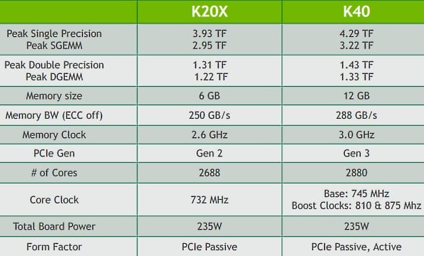
Just as the GTX 780 Ti was the full consumer implementation of the GK110 GPU, the new K40 Tesla card is the supercomputing / HPC variant of the same core architecture. The K40 picks up additional clock headroom and implements the same variable clock speed threshold that has characterized Nvidia's consumer cards for the past year, for a significant overall boost in performance.

According to Nvidia, it hasn't had to raise the thermal threshold for the card at all; both the K20X and K40 are 235W solutions. This implies that either the K20 was over-rated on power or NV has had very good luck with improving GK110's yields and power consumption. Either is possible, since we know that semiconductor manufacturers typically see a 10-15% power consumption improvement from the beginning to the end of a process generation and 28nm is a mature process at this point.
The other major shift between the K20X and the K40 is the amount of on-board RAM. K40 packs a full 12GB and clocks it modestly higher to boot. That's important because datasets are typically limited to on-board GPU memory (at least, if you want to work with any kind of speed). Doubling K20X's RAM opens up new kinds of problems and will compete well against Intel's Knights Corner / Knights Landing. But that's not the only change to the K40's memory structure that Nvidia is announcing. The new version of CUDA the company is prepping, CUDA 6, uses a unified memory model.
Understanding what CUDA 6 does and doesn't do takes a bit of explanation. First off, this slide looks very similar to some of the high-level HSA diagrams AMD has shown. So if CUDA 6 can do unified memory addressing, why has AMD pursued a route that requires specific additional hardware to implement? The short answer is that Nvidia has built a software model that simplifies the task of attempting to unify memory between CPU and GPU -- CUDA can now do this automatically in software.
The downside to a software implementation is that it might not be as fast depending on the call/workload -- all of the bandwidth and latency issues you'd expect to exist between the relatively pokey PCIe 3.0 bus (by DRAM standards) and main memory still exist. Still, this is an important step for programmers, who don't have to try to handle the task themselves if they need to share data. Maxwell will be the first Nvidia GPU with hardware-level support for unified virtual memory, which means we should see a performance improvement in this mode with next-gen GPUs. Getting the code lined up now, however, is still important.
According to Nvidia's release, Tesla GPUs will ship alongside Power8 CPUs, which are currently scheduled for a mid-2014 release date. We haven't talked much about Power8, but the next iteration of IBM's venerable architecture is expected to target a 4GHz clock speed and offer up to 12 cores, with 96KB of L1 and 512K of L2 per core and 96MB of L3 on the entire chip. A 12-core implementation would be capable of handling up to 96 simultaneous threads (eight threads per core). The next-generation chip is targeting 2-3x Power7's performance and will be built on a 22nm process. No doubt, the combined solution should be seriously robust and very competitive versus alternative platforms.
K40 -- GK110 Goes Full Fat
Just as the GTX 780 Ti was the full consumer implementation of the GK110 GPU, the new K40 Tesla card is the supercomputing / HPC variant of the same core architecture. The K40 picks up additional clock headroom and implements the same variable clock speed threshold that has characterized Nvidia's consumer cards for the past year, for a significant overall boost in performance.
According to Nvidia, it hasn't had to raise the thermal threshold for the card at all; both the K20X and K40 are 235W solutions. This implies that either the K20 was over-rated on power or NV has had very good luck with improving GK110's yields and power consumption. Either is possible, since we know that semiconductor manufacturers typically see a 10-15% power consumption improvement from the beginning to the end of a process generation and 28nm is a mature process at this point.
The other major shift between the K20X and the K40 is the amount of on-board RAM. K40 packs a full 12GB and clocks it modestly higher to boot. That's important because datasets are typically limited to on-board GPU memory (at least, if you want to work with any kind of speed). Doubling K20X's RAM opens up new kinds of problems and will compete well against Intel's Knights Corner / Knights Landing. But that's not the only change to the K40's memory structure that Nvidia is announcing. The new version of CUDA the company is prepping, CUDA 6, uses a unified memory model.

Understanding what CUDA 6 does and doesn't do takes a bit of explanation. First off, this slide looks very similar to some of the high-level HSA diagrams AMD has shown. So if CUDA 6 can do unified memory addressing, why has AMD pursued a route that requires specific additional hardware to implement? The short answer is that Nvidia has built a software model that simplifies the task of attempting to unify memory between CPU and GPU -- CUDA can now do this automatically in software.
The downside to a software implementation is that it might not be as fast depending on the call/workload -- all of the bandwidth and latency issues you'd expect to exist between the relatively pokey PCIe 3.0 bus (by DRAM standards) and main memory still exist. Still, this is an important step for programmers, who don't have to try to handle the task themselves if they need to share data. Maxwell will be the first Nvidia GPU with hardware-level support for unified virtual memory, which means we should see a performance improvement in this mode with next-gen GPUs. Getting the code lined up now, however, is still important.
IBM Collaboration
The other major announcement of the day is an IBM-Nvidia partnership to combine Tesla GPUs and Power CPUs. The goal is to push the new Tesla cards as workload accelerators for specific datacenter tasks. Nvidia had previously joined the OpenPower consortium, which opened IBM's Power architecture up for licensing and broad adoption to various interested parties. This move advances Nvidia's goal of pushing CUDA into more high-end, big iron deployments where Power servers are still well represented.
According to Nvidia's release, Tesla GPUs will ship alongside Power8 CPUs, which are currently scheduled for a mid-2014 release date. We haven't talked much about Power8, but the next iteration of IBM's venerable architecture is expected to target a 4GHz clock speed and offer up to 12 cores, with 96KB of L1 and 512K of L2 per core and 96MB of L3 on the entire chip. A 12-core implementation would be capable of handling up to 96 simultaneous threads (eight threads per core). The next-generation chip is targeting 2-3x Power7's performance and will be built on a 22nm process. No doubt, the combined solution should be seriously robust and very competitive versus alternative platforms.