Samsung Headed For 14nm Semiconductor Manufacturing Milestone With ARM
At this rate, one has to wonder if die sizes won't be infinitesimal in 10 years. As process technology improvements continue to enable SoC makers to create smaller and smaller chips with more and more power, Samsung has been at the forefront of the push. Now, Synopsys has announced that its multi-year collaboration with Samsung on FinFET technology has led to a major milestone: the successful tapeout of the first test chip on Samsung's 14LPE process.
There's no clear word on when this innovation will actually be available for mainstream use, but it'll no doubt make our smaller gadgets of the future a heck of a lot more potent.
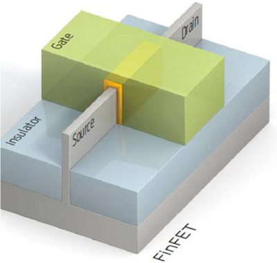
While the FinFET process offers significant power and performance benefits compared to the traditional planar process, the move from two-dimensional transistors to three-dimensional transistors introduces several new IP and EDA tool challenges such as modeling. The multi-year collaboration delivered the foundational modeling technologies for 3D parasitic extraction, circuit simulation and physical design-rule support of FinFET devices. Synopsys' comprehensive solution for embedded memory, physical design, parasitic extraction, timing analysis and signoff is built on this foundation.
Synopsys worked closely with Samsung to develop a test chip that validates Samsung's advanced 14-nm FinFET process as well as Synopsys' DesignWare Embedded Memories using Synopsys' Self-Test and Repair (STAR) Memory System solution. The test chip will enable the correlation of the simulation models to the FinFET process and contains test structures, standard cells, a PLL and embedded SRAMs. The memory instances include high-density SRAMs designed to operate at very low voltages and high-speed SRAMs to validate the process performance.
There's no clear word on when this innovation will actually be available for mainstream use, but it'll no doubt make our smaller gadgets of the future a heck of a lot more potent.